Table Of Content
Speaking of sharing, for an in-depth discussion of many diverse types of EDA tools and how AMD performance improvements deliver tangible benefits to EDA customers, see the latest blog on EPYC CPUs excelling at EDA workloads from Raghu Nambiar. As a student passionate about electronic design and the semiconductor industry, I attend DAC to get a head start on my career. I am able to demonstrate my skills to design professionals and connect with mentors, recruiters, and future colleagues worldwide. I know that DAC can jumpstart careers by providing unparalleled networking and recruitment opportunities. However, due to the relative simplicity of the ML techniques adopted, they are not able to train ML models that can consider rich semantics in code or learn from historical bug fixes.
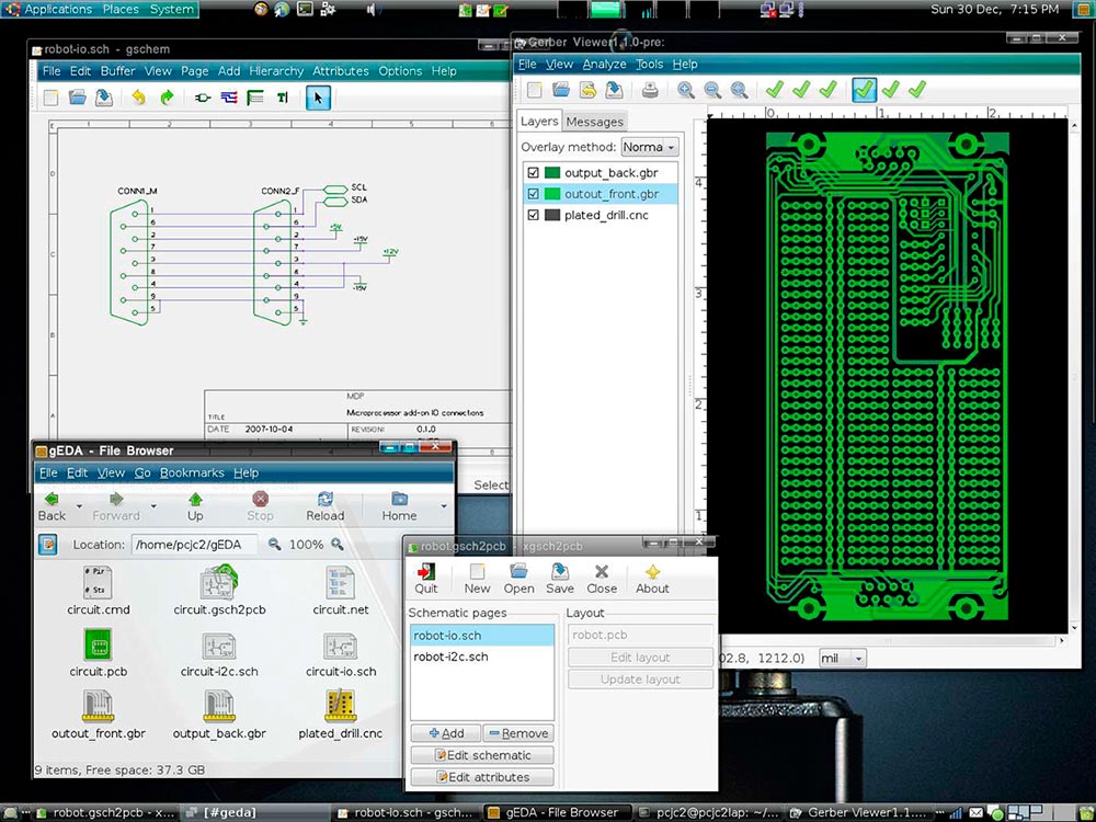
Static code analysis
In our experience running datacenters and cloud environments for many years, AMD EPYC processors have turned out to be the best bet to tackle the diversity of EDA demands. The highest frequency AMD EPYC 9004 CPUs can be paired with very large memory to deliver faster execution times for heavy duty, compute-driven workloads. EPYC 9004 series processors with 3D V-Cache technology can deliver significant performance increases for technical computing applications and high throughput verification workloads .
Partner Solutions
Most recently he served as the Corporate Vice President of Research and Advanced Development at AMD. During his tenure at the company, he founded AMD Research where he oversaw the company’s worldwide research and advanced technology labs, university engagements, and external research contracting. Alan also led extreme-scale computing technology at AMD, where he drove the software and hardware engineering efforts to build the world’s fastest platforms for machine learning, industrial, and scientific applications. Electronics manufacturing organizations require increasing amounts of compute and storage for electronic design automation (EDA).
What Is the Future of Electronic Design Automation and How Are EDA Tools Adapting?

The semiconductor ecosystem today can be seen as a triangle, says Mike Demler, a consultant who has been in the chip design and EDA industry for over 40 years. On one corner are the foundries, or chip manufacturers like TSMC; on another corner are intellectual-property companies like ARM, which make and sell reusable design units or layouts; and on the third corner are the EDA tools. EDA is the most upstream and high-end industry in the integrated circuit industry chain in the semiconductor industry, the cornerstone of chip design, and one of the crucial support mechanisms for chip design innovation. Electronic design automation tools and processes have been a part of the semiconductor industry for more than 60 years.
Support
Learn how SiTime leverages AFS, Symphony and Solido Design Environment to ensure seamless integration between the analog and digital components and accelerate verification of high precision MEMS based oscillators SoC. Today, AMD is at the leading edge of the AI wave, in providing CPU solutions for ML and AI inference. Three progressive problems need to be solved to speed up bug hunting in functional verification, namely, clustering of bugs by their root causes, classification of root causes, and suggestion of fixes. Most research focuses on the first two, with no research results on the third one available yet. In its latest five-year plan, which is the country’s top economic blueprint, EDA was listed as the first cutting-edge technology within the semiconductor industry where China needs to make breakthroughs.
Electronic design automation (EDA) refers to a consortium of computer software tools that help with the design, production, packaging, and testing of large-scale integrated circuit chips. EDA developed in the middle of the 1960s from the ideas of computer-aided design (CAD), computer-aided manufacturing (CAM), computer-aided testing (CAT), and computer-aided engineering (CAE). Accurate data acquisition and system modeling are the foundations of effective electronic design automation. For example, specific MIPI standards models are required to perform circuit board design verifications, like compliance testing of MIPI boards, that are used in displays for everything from smartphones to automobiles to industrial systems. The global electronics supply chain has been disrupted due to the ongoing Russia-Ukraine war.
Learn more about Siemens EDA
SNS Insider has been a leader in data and analytics globally with its authentic consumer and market insights. The trust of our clients and business partners has always been at the center of who we are as a company. The electronics industry's relentless push for sophistication and miniaturization is fueling a surge in demand for advanced EDA tools.
How Modern Packaging is Reshaping the Future of Electronics

Research has proven that smell detection with ML can lead to universal code smell detection and significantly fewer pattern implementation efforts. The resulting smell score can then be used for code quality assessment and help developers improve product quality consistently. Furthermore, ML-based code refactoring might provide helpful hints on improving code smell or even further some candidate changes. The advance of ML translation in the NL domain has made fully-automated machine translation commercially feasible and sometimes exceeds the performance of average human translators. Several attempts to do a successful end-to-end translation have been observed, but none have been made production ready. The major hurdle to this approach is the scarcity of available training datasets that pair NL specifications with their formal translation.
Additionally, Helix IPLM can help semiconductor organizations ensure that they meet fab security requirements by providing a single source of truth that teams can use to establish a versioned, hierarchical bill of materials. Veloce CS is the leading hardware software and system validation platform, including the Veloce Strato CS emulation platform, Veloce Primo CS enterprise prototyping platform, and Veloce proFPGA CS software prototyping platform. Bell Laboratories, Texas Instruments, Intel, RCA, General Electric, Sony, and Sharp are examples of these companies. While the on-premise EDA segment holds the dominant market share due to factors like data security and customizability, the cloud-based segment is experiencing rapid growth because of its cost-effectiveness and scalability. In this presentation we share how we worked with a customer to migrate from a sophisticated array of home-grown spreadsheets and scripts to process and coverage analysis automation with Questa Verification IQ.
Notably, the advent of EDA 1.0 was ushered in by the introduction of SPICE (simulation program with integrated circuit emphasis) at the University of California, Berkeley, in the early 1970s, which revolutionized circuit design. The restricted tools are those that can be used for GAAFET (gate-all-around field-effect transistor) architecture, the most advanced circuit structure today, which is critical to making the latest chips and more advanced ones in the future. The Commerce Department is still seeking public comment to identify which EDA software is most helpful in achieving this specific structure and therefore should be added to the list. Front-end logic design and back-end physical design make up the bulk of it, and front-end designers and back-end designers typically play different roles on teams. Front-end design and back-end design are typically separated by the generated gate-level netlist, despite the lack of a standard and distinct boundary.
Electronic design automation is a response to these high stakes and lets semiconductor teams test designs before they are manufactured. EDA software empowers teams to predict how chips will perform over time, letting semiconductor professionals measure chip reliability even before production. Modern semiconductor technology would be impossible without a high level of electronic design automation. In fact, EDA tools now power an increasingly wide array of industries, from automotive and consumer electronics to aerospace technology and telecommunications. EMA Design Automation is a leading provider of the resources that engineers rely on to accelerate innovation. Based on decades of engineering expertise, we provide solutions that include cutting edge PCB design and analysis packages and customized integrations to help you optimize your electronic development workflow and create more efficiently.
DAC 2023, Day 1: Design Automation in the Age of AI - EE Times
DAC 2023, Day 1: Design Automation in the Age of AI.
Posted: Tue, 11 Jul 2023 13:14:54 GMT [source]
Welcome to the era of EDA 4.0, where we are witnessing a revolutionary transformation in electronic design automation driven by the power of artificial intelligence. The history of EDA can be delineated into distinct periods marked by significant technological advancements that have propelled faster design iterations, improved productivity, and furthered the development of intricate electronic systems. In the short term China won’t be that badly affected, because Chinese foundries are not advanced enough to make the state-of-the-art chips that need the GAAFET structure. But the blockade means Chinese chip design firms won’t be able to access the most advanced tools, and as time passes, they’ll most likely fall behind.
Many semiconductor professionals wonder how EDA tools and the companies that create and support them will adapt to geopolitical events, the rise of new technology, and other changes. Along with using electronic design automation software, using an IP-centric approach can empower your team to work more efficiently. Our Transformation Model for IP-Centric Design white paper details how placing IP at the center of your design process can help you get to market faster than the competition and reduce costly re-spins. Plus, it breaks down the five-step process to follow to achieve this transformation. Siemens EDA is a leader in the development of complete flows for the design, verification and manufacturing of printed circuit boards.
After the fab has finished designing semiconductor devices and manufacturing processes, it must use EDA tools to create PDKs, standard cell libraries, and IPs. Lithography calculations and yield enhancement during the wafer manufacturing process are also tasks that must be completed using EDA software tools. Device model extraction tools, process and device simulation (TCAD), PDK development and verification, computational lithography, mask calibration, mask synthesis, and yield analysis are examples of wafer fabrication EDA tools. Since semiconductor design comes with complex challenges and high stakes – including strict regulations, tight time-to-market timelines, and an immense cost of error – teams need strong, trusted design tools.
AMD Engineering and IT organizations work together to continuously test and improve the AMD EPYC processor-powered datacenter for every major type of workloads, including EDA. Although theoretically the same ML techniques applied to other programming languages can be applied to IC design, no research has been published yet on coding assistance. The other group leverages the classic natural language process (NLP) to parse NL specifications and extract relevant key elements to formulate formal specifications. The Chinese government may have been tough on consumer tech platforms, but its AI regulations are intentionally lax to keep the domestic industry growing.
Foster is the recipient of the Accellera Technical Excellence Award for his contributions to developing industry standards and was the original creator of the Accellera Open Verification Library (OVL) standard. In addition, Foster is the recipient of the 2022 ACM Distinguished Service Award, and the 2022 IEEE CEDA Outstanding Service Award. Converse to requirement definition, summarization looks at the code and translates it into a human-understandable NL summary. It assists developers in reading less ideally maintained code or understanding complex logic.


No comments:
Post a Comment